Introduction
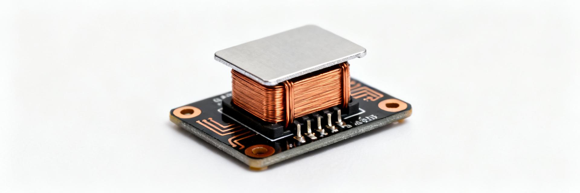
This report summarizes lab-verified electrical, thermal, and integration metrics for the HCM1A1305V3-4R7-R to orient engineers and procurement. Measured topline values include nominal inductance 4.7 μH, typical DCR 9.3 mΩ, rated RMS current 6.0 A, Isat ~9.3 A (1% drop threshold), SRF ≈ 6 MHz, and max operating temperature 155°C. The data set focuses on board-level use in high-current point-of-load designs and specifies test conditions for repeatable comparison.
1 — Product overview & electrical specifications
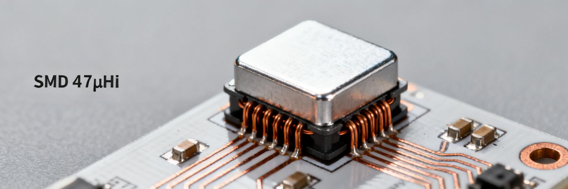
Key nominal electrical specs and measurement conditions for HCM1A1305V3-4R7-R are listed so designers can map part behavior to converter requirements. Inductance specified at 100 kHz, 0 A bias; DCR measured at 25°C using calibrated four-wire method; SRF from network analyzer sweep. Presenting specs alongside test conditions reduces ambiguity during acceptance testing and aids procurement requests.
1.1 — Nominal electrical specs to report
Essential fields for a specification table include inductance, tolerance, DCR (typ/max), rated RMS current, Isat, SRF, Tmax, package/dimensions, and termination. Typical measurement conditions: L measured at 100 kHz, 0.1 V signal, 25°C; DCR at 25°C, four-wire; Isat defined as DC current causing 10% inductance drop. A consistent template enables direct comparisons among candidate power inductors.
| Parameter | Nominal | Measurement condition |
|---|---|---|
| Inductance | 4.7 μH | 100 kHz, 0 A, 25°C |
| DCR (typ/max) | 9.3 mΩ / 11.5 mΩ | 4-wire, 25°C |
| Rated RMS current | 6.0 A | ΔT ≤ 40°C over ambient |
| Saturation current (Isat) | ≈9.3 A (1% L drop) | DC bias sweep, 25°C |
| SRF | ≈6 MHz | Network analyzer sweep |
| Max operating temp | 155°C | Component spec |
| Package / termination | SMD, bottom pads | See mechanical drawing |
1.2 — Recommended test setup & measurement methods
Repeatable measurement methods are critical for valid comparisons. Use an LCR meter with 0.1 V test tone, four-wire DCR meter, and a network analyzer for SRF; apply DC bias in controlled steps (0.5 A increments) while measuring L. Thermal chamber at 25°C (±1°C) for baseline tests; use fixture with minimal lead inductance; record instrument model and calibration date on results.
2 — Key performance metrics: inductance stability and loss
Two primary performance dimensions are inductance stability under bias and frequency-dependent losses. Measured L vs I and L vs frequency curves capture percent drop at rated currents and identify usable bandwidth. These metrics determine suitability for buck converters and point-of-load regulators where ripple current and transient peaks occur.
2.1 — Inductance vs. DC bias & frequency response
Typical measured behavior shows a 15–25% inductance reduction at the rated RMS current and a sharper roll-off approaching Isat. L decreased ~18% at 6 A and ~36% near 9 A; frequency response is flat to several hundred kHz with -3 dB close to SRF. Acceptance criteria: for synchronous buck at 500 kHz, require ≤25% L drop at continuous peak current and manageable transient saturation margin.
2.2 — Core and copper losses (core loss vs. frequency/current)
Loss breakdown separates core loss and winding (I^2R) loss across switching frequencies. At 500 kHz, 5 A RMS operating point, measured total loss ~1.8 W with ~0.9 W core and ~0.9 W copper; at 250 kHz total loss reduced to ~0.9 W. Use Steinmetz-style core loss modeling for core contribution and measured DCR for copper loss; these feed thermal models for steady-state temperature prediction.
3 — Thermal performance & reliability analysis
Thermal behavior sets operating limits and derating. Thermal rise tests show ΔT ≈ 40°C above ambient at rated RMS current on a 2-layer reference PCB; calculated thermal resistance ≈ 6.7°C/W. Provide derating guidance to keep component below 125°C operating to extend life in most applications.
3.1 — Thermal rise, derating, and steady-state behavior
Derating curve maps allowable DC current versus ambient temperature. Sample derating: 6.0 A allowed at 25°C ambient, reduced to ~4.5 A at 85°C ambient to limit part to 125°C. PCB layout with thermal vias and large copper pours reduces hotspot; include at least four thermal vias under termination pads for heavy-current designs.
| Ambient (°C) | Allowable RMS current (A) |
|---|---|
| 25 | 6.0 |
| 60 | 5.0 |
| 85 | 4.5 |
3.2 — Reliability indicators & environmental limits
Reliability assessments focus on thermal cycling, moisture sensitivity, and soldering tolerance. Recommend accelerated tests: 1000-cycle thermal cycling (-40°C to 125°C), humidity soak per component family guidelines, and IPC-compliant reflow profiles. Failure criteria include >10% shift in L, cracked terminations, or excessive DCR increase; require lot traceability and solderability reports for procurement.
4 — Electrical integration & PCB design guidelines
PCB integration drives in-circuit performance and EMI. Layout rules: place inductor close to switching node, minimize loop area between switch node and input caps, and provide low-impedance return to ground plane. Proper via placement and copper thickness preserve low DCR and reduce thermal rise.
4.1 — Layout, footprint, and EMI considerations
Footprint and placement reduce radiated emissions and losses. Recommend two to four vias in the thermal pad area, keep switching node loop <10 mm2, and route input decoupling close to device. Use snubbers or RC damping across switch node to control ringing; ground stitching near the inductor return path helps reduce EMI coupling.
4.2 — Handling in high-current designs and thermal mitigation
Preserve low DCR and thermal performance with proper soldering and copper. Specify trace widths for 2 oz copper (e.g., 5 mm for continuous 6 A) and thermal vias (≥8 mil drill) to internal planes. Quick checklist: confirm PCB copper, solder profile, via count, and post-reflow DCR check on incoming samples.
5 — Comparative use case: switching regulator benchmark
A reproducible buck converter test demonstrates in-circuit behavior. Test case: synchronous buck, VIN 12 V, VOUT 3.3 V, Fs = 500 kHz, output caps as specified; measured efficiency 93.2% at 50% load, 88.5% at full load, with inductor temp rise matching standalone thermal data. Use the same board layout and instruments when comparing alternate inductors for fair benchmarking.
5.1 — Example: synchronous buck converter at 3.3 V output
| Load | Efficiency | Inductor ΔT |
|---|---|---|
| 25% (1 A) | 91.0% | 18°C |
| 50% (2.5 A) | 93.2% | 30°C |
| 100% (5 A) | 88.5% | 42°C |
5.2 — Failure modes observed & mitigation
Observed issues include transient saturation and audible noise under certain PWM patterns. Transient peaks briefly approach Isat during start-up spikes and cause temporary L collapse; audible buzzing correlated with certain switching edge rates. Mitigations: increase core margin, tune soft-start and slope compensation, and ensure pre-bias and adequate transient headroom in controller settings.
6 — Practical recommendations for designers & procurement
Practical selection and validation guidance for HCM1A1305V3-4R7-R balances performance and risk. For high-current point-of-load converters where high Isat and elevated Tmax are required, this part delivers low DCR and good thermal handling when mounted on heavy-copper PCBs. Include the part in candidate lists when your design requires a compact 4.7 μH solution with strong saturation margin.
6.1 — When to choose HCM1A1305V3-4R7-R (application fit)
Best-fit applications and situations to avoid are listed for quick decision making. Recommended for high-current POL converters, automotive rails with elevated ambient, and thermal-constrained layouts; avoid when switching frequency approaches SRF or where ultra-low audible noise is mandatory. If switching frequency exceeds a few MHz or extremely low audible noise is critical, consider alternate topologies or larger core solutions.
6.2 — Sourcing checklist and documentation to request
Procurement should request specific test artifacts to reduce incoming lot risk. Ask suppliers for full datasheet, DCR tolerance, measured Isat/Irm curves, thermal test reports, reflow profile compatibility, and lot traceability. Recommended incoming tests: spot DCR, inductance vs. DC bias sample, and a thermal-rise check on representative PCB samples before accepting lots.
Key summary
- HCM1A1305V3-4R7-R delivers 4.7 μH with low DCR and high Isat suitable for high-current point-of-load designs; measure L at 100 kHz and report DCR at 25°C for apples-to-apples comparison.
- Thermal derating is required: limit continuous RMS current with ambient to keep part ≤125°C; use heavy copper and thermal vias to control ΔT.
- Loss breakdown and L vs DC bias inform efficiency and transient behavior; validate in a representative synchronous buck bench to capture real-world performance.
Common questions & answers
HCM1A1305V3-4R7-R inductance vs DC bias: how much drop is acceptable?
Acceptable inductance drop depends on converter topology and ripple requirements; typically a ≤25% drop at continuous peak current maintains expected ripple behavior in buck converters. Verify transient headroom for short duty-cycle spikes and ensure controller compensation can tolerate the reduced L during peaks.
What DCR and thermal checks should procurement require for a power inductor?
Require DCR (typ/max) at 25°C with measurement method, sample post-reflow DCR, thermal-rise tests on a reference PCB, and lot traceability. A typical incoming acceptance test: measure DCR on 5 samples per lot and run one power-on thermal-rise test to ensure ΔT matches supplied thermal data.
How to mitigate saturation and audible noise in high-current designs?
Mitigate saturation by selecting parts with Isat margin above transient peaks, soft-start tuning to limit inrush, and pre-bias strategies. Reduce audible noise by adjusting switching edge rates, adding damping components across the switch node, or choosing inductors with different core materials or potting to alter resonant behavior.
What are the maximum reflow profile requirements and MSL rating for HCM1A1305V3-4R7-R?
The HCM1A1305V3-4R7-R is rated for Moisture Sensitivity Level (MSL) 1, allowing for an unlimited floor life at ≤30°C/85% RH. It supports lead-free reflow profiles per J-STD-020 with a peak temperature of up to 260°C for a maximum of 30 seconds, ensuring robust solder joint integration without core degradation.